1. Why Now — The Copper Wall
At 224G SerDes, copper traces inside chips are hitting a power wall. The energy to push electrons through shrinking wires is growing faster than bandwidth. Intel, Broadcom, NVIDIA, AMD, and Cisco are already shipping silicon photonics in data centers — replacing electrical interconnects with waveguides that carry light.
This is not a research curiosity anymore. It is production silicon. And every one of those photonic chips has a digital controller at its heart — a calibration FSM, a heater DAC, a wavelength lock loop — written in the same SystemVerilog you already know.
The boundary between that digital controller and the photonic physics introduces verification challenges that existing workflows were not designed for. When a photonic respin in a hyperscale AI chip can cost tens of millions of dollars and delay a product launch by a year, those challenges become worth solving systematically.
We started exploring this a few months ago. We are not photonics physicists. We are verification engineers — RTL, gate-level, fault injection, coverage-driven methodology. When we looked at how photonic links are verified today, we saw an opportunity to extend familiar disciplines into a new domain.
2. Two Worlds, Same Problem
If you verify chips for a living, you know the picture on the left. RTL goes through synthesis, becomes gates, gets simulated and checked. You have done this many times.
Now look at the right side. That is a photonic link — data traveling as light through a chip instead of electrons through copper. Different physics. But look at the structure. It is the same engineering pattern: something generates a signal, something carries it, something receives it, and a controller keeps everything stable.
The left side uses electrons. The right side uses photons. But the bottom three blocks on both sides — the PLL, the DAC, the FSM — are pure digital. Written in SystemVerilog. Synthesized to gates. Verified with the same tools you already use.
The physics changed. The engineering did not. Drift, calibration, fault recovery, corner cases — it is the same discipline with a different signal domain.
3. The Boundary Challenge
In a typical photonic chip development, the digital team writes the control FSM — calibration, wavelength locking, thermal tuning, fault recovery. They simulate it against a model of the optical output. The photonics team designs the optical components and simulates light behavior in specialized tools against an idealized control signal.
Both teams do rigorous work within their domains. The challenge is at the boundary. The controller and the photonic device interact through a continuous feedback loop — DAC codes driving thermal tuning, photocurrent feeding back to the FSM — and that interaction is difficult to capture when each domain is verified separately.
Excellent optical tools exist for photonic device simulation. Excellent digital tools exist for controller verification. The challenge is running them together in a single closed-loop simulation where the digital controller drives the photonic physics and the photonic physics drives the digital controller — every cycle, every interaction, every corner.
We decided to build a bridge.
4. What We Built — A Starting Point
We built a mixed-domain co-simulation framework. Not a finished product — a working foundation. Digital gate-level simulation driving photonic behavioral models through DAC/ADC boundaries. Closed loop. One simulation.
The top row is familiar territory — RTL through synthesis, gates simulated cycle-accurate. The bottom row is the optical domain — behavioral models that capture the physics relevant to verification: loss, drift, noise, coupling.
The boundary is explicit. DAC codes go down. Photocurrent comes back up. Same as real hardware. The FSM does not know it is talking to a model. The model does not know it is driven by gates. They just exchange signals every clock cycle.
5. The Device Models — Familiar Abstractions
Think of these as behavioral models at the verification abstraction level — like Verilog-A models for analog blocks. Real enough to catch integration bugs. Fast enough to run regressions.
| Device | What it does | Digital equivalent |
|---|---|---|
| Ring Modulator | Switches light on/off by tuning a resonant ring | PLL / tunable oscillator |
| MZI Modulator | Splits light, phase-shifts, recombines | Differential driver |
| Photodiode | Converts light back to electrical current | ADC front-end |
| Waveguide | Carries light on-chip with propagation loss | Metal wire with RC delay |
| Grating Coupler | Gets light on and off the chip | Bond pad |
| Heater / DAC | Electrically tunes the ring wavelength | Trim DAC |
Each model is parameterized from YAML configuration — the photonic equivalent of a .lib file. Change the coupling coefficient, propagation loss, or photodiode responsivity, and the entire link responds consistently. The models include PVT-aware thermal coefficients, laser RIN noise, and receiver shot noise — the parameters that affect controller behavior at the digital-optical boundary.
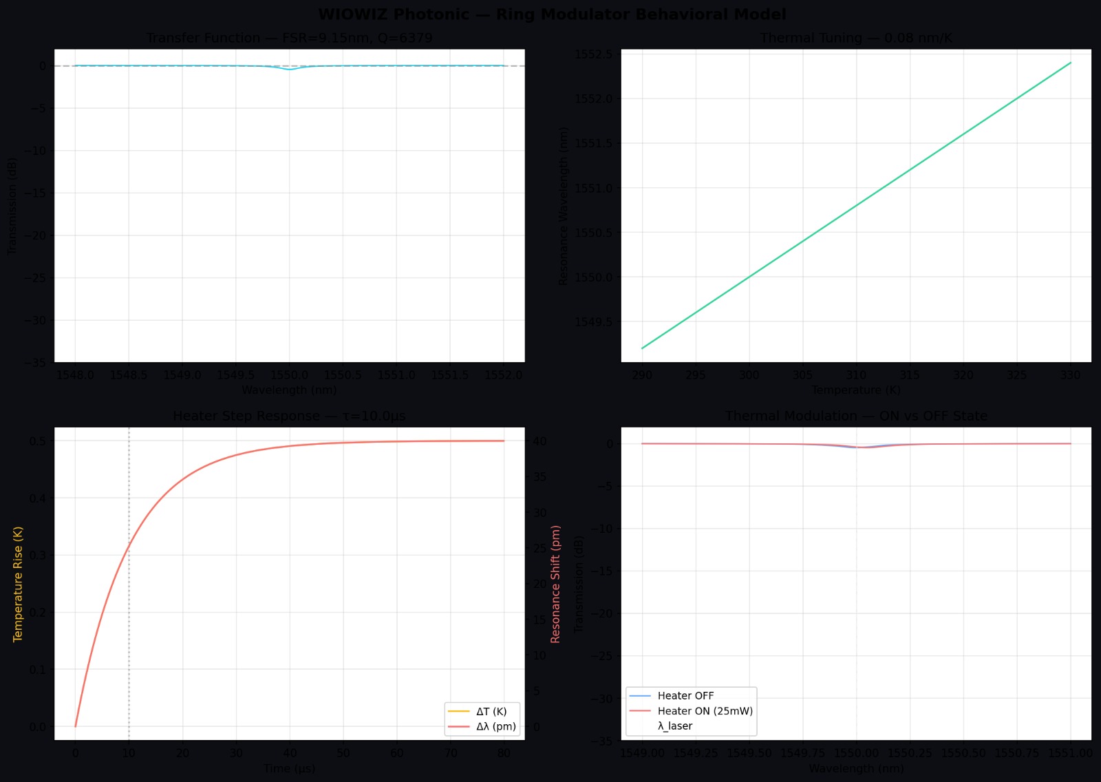
Here is what the ring modulator model produces. Four panels: the Lorentzian transfer function showing the resonance notch, thermal tuning response across temperature, heater step response with first-order settling, and the modulation states showing on/off wavelength positions.
6. The Control FSM — Pure Digital
The calibration controller is a 6-state FSM. Written in synthesizable SystemVerilog. If you have written state machines for SERDES initialization or DDR training sequences, this will feel very natural.
Yosys synthesizes it to gates. Our VHE engine simulates the gate-level netlist cycle-accurate. The FSM drives the heater DAC, the photonic link computes the optical response, the photodiode converts to photocurrent, and the FSM reads it back.
In our tests, the FSM goes RESET → CALIBRATE → LOCK → MONITOR, converges, and holds stable for tens of thousands of cycles. The Python golden model and C gate-level engine produce matching results.
7. Fault Injection — Because Happy Path Means Nothing
Any verification engineer knows: the design works perfectly until something breaks. We run fault scenarios through the full co-simulation loop.
| What breaks | How we simulate it | What should happen |
|---|---|---|
| Heater stuck at max | Force DAC full scale | FSM detects and enters FAULT |
| Wavelength jumps | Instant shift in ring resonance | RELOCK sequence recovers |
| Temperature drifts | Slow thermal ramp | FSM tracks continuously |
| Fiber disconnected | Photodiode goes dark | FAULT state, safe shutdown |
| Fiber re-plugged | Signal returns with new loss | Recalibrate and reacquire |
| Power supply dips | Reduced drive voltage | Re-tune without false alarm |
This is the same discipline — fault injection, coverage analysis, corner-case hunting — applied to a domain where most teams still rely on bench testing.
8. BER and Eye Diagrams — The Language Photonics Engineers Speak
When a photonic engineer asks "does your link work?" — the answer is a BER number and an eye diagram. It is the equivalent of "does your chip meet timing?"
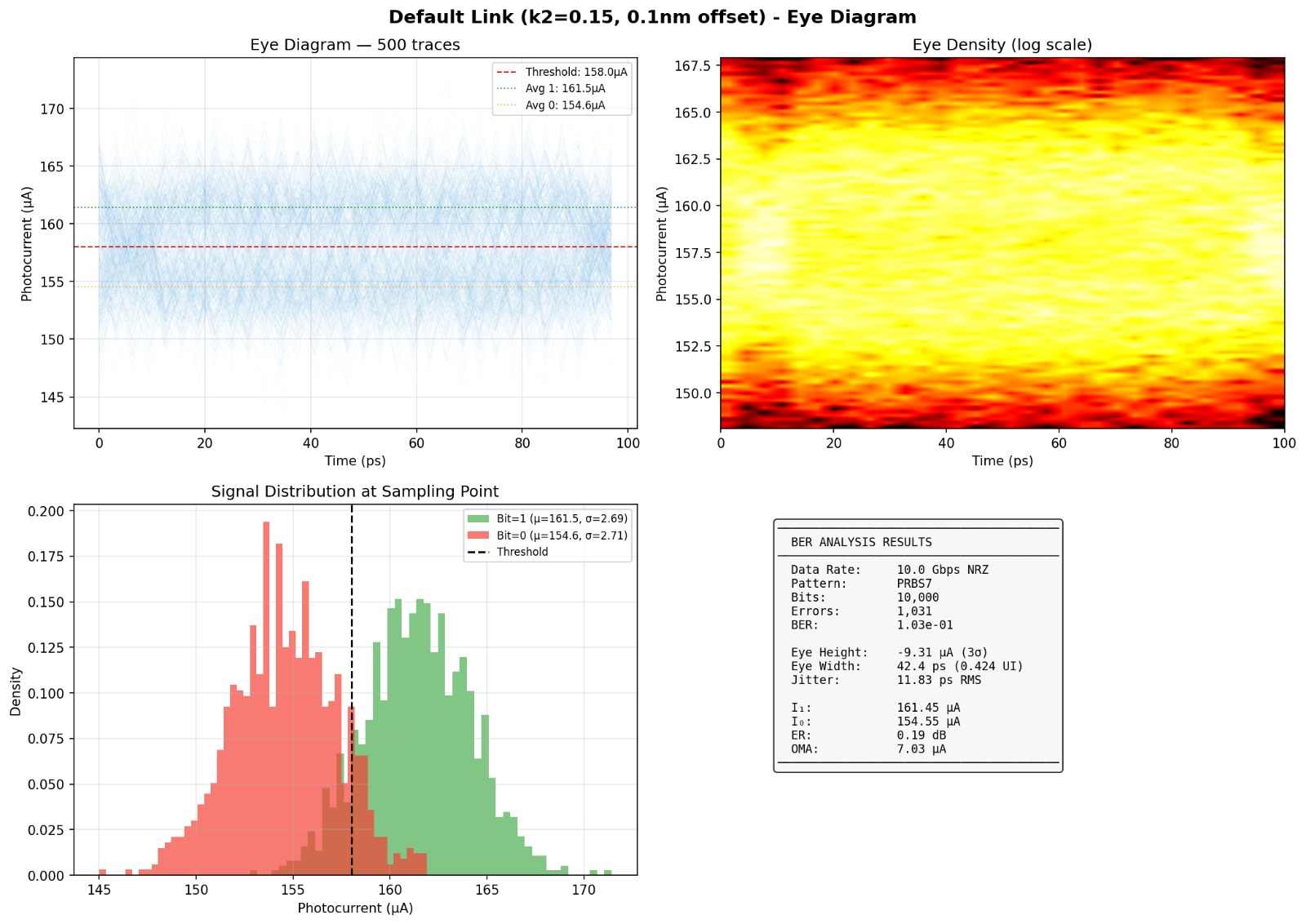
We built a BER estimation engine that transmits real bit patterns (PRBS-7 per ITU-T O.150) through the full photonic link model. Each bit goes through the ring modulator, waveguide, and photodiode — with real noise from the receiver model. The engine computes both statistical BER (Gaussian approximation via Q-factor) and direct BER (brute-force bit counting with bathtub curve characteristics), then generates eye diagrams.
Here is the eye diagram from a default configuration run. The eye is nearly closed — the two signal distributions overlap heavily, giving a BER of about 10%. This is expected: the ring modulator coupling is far from optimal.
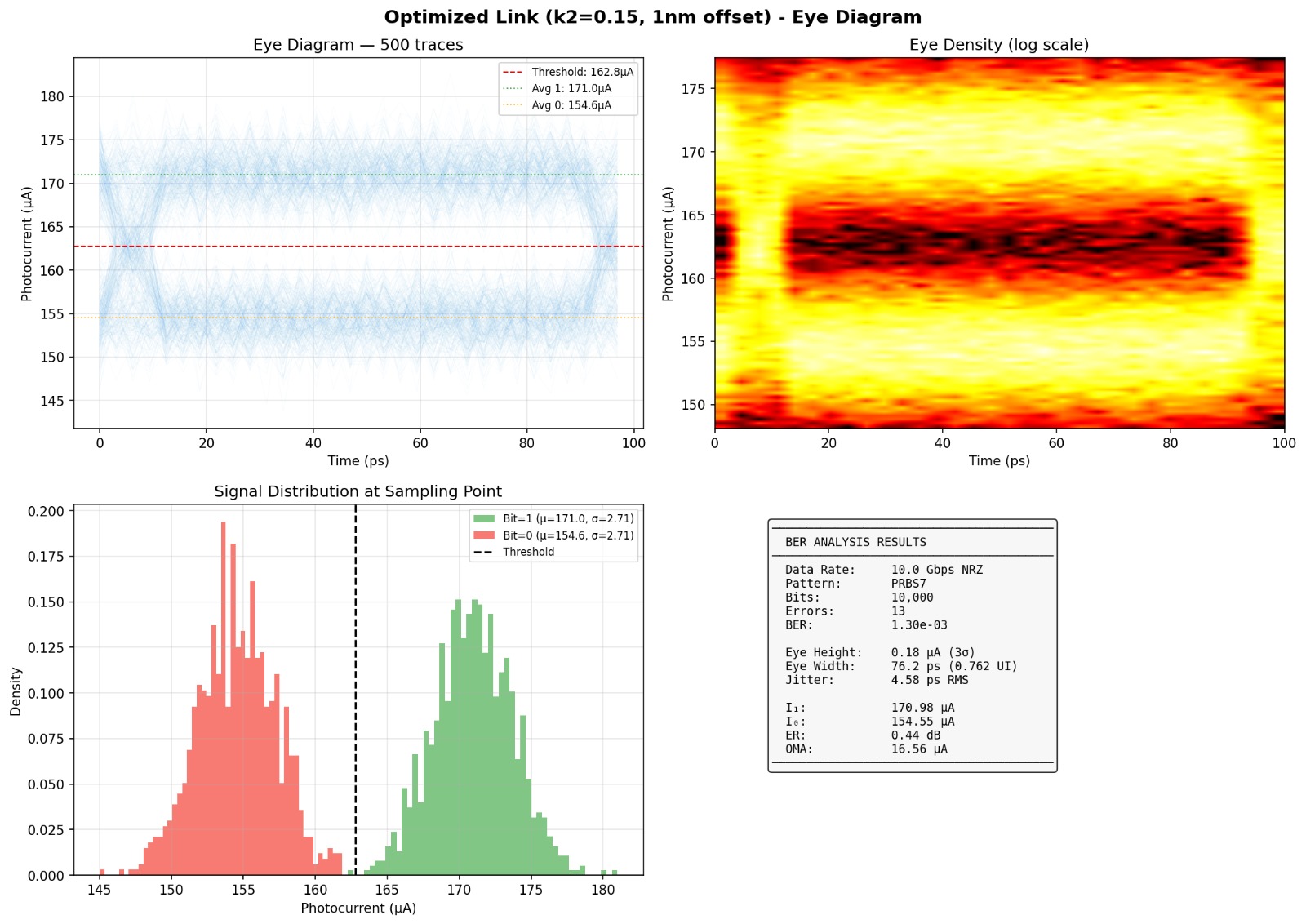
Now here is the same link with optimized wavelength offset. The eye opens — two distinct signal levels appear, the histograms separate, and the BER drops by two orders of magnitude.
The entire flow runs from a single YAML configuration file. One command produces: link characterization, BER analysis (statistical and direct), fault injection results, parameter sweeps, eye diagrams, and a JSON report.
Verification run — actual results
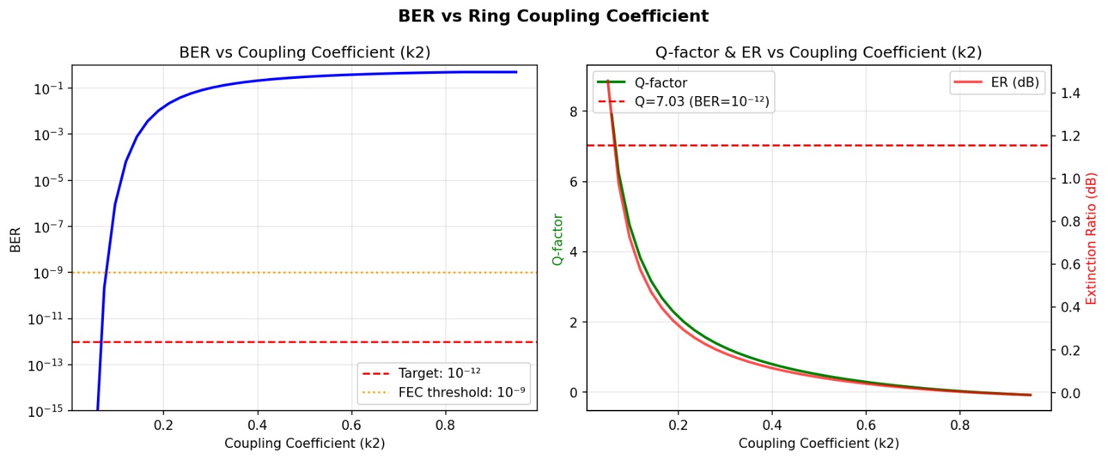
The coupling sweep is particularly revealing. By varying the ring modulator coupling coefficient from κ²=0.05 to 0.6, BER spans fifteen orders of magnitude — from 3.87×10⁻¹⁹ (well below the 10−12 target) to 0.39 (essentially random). The framework finds the optimal operating point automatically — something that would require days of lab measurement on real hardware.
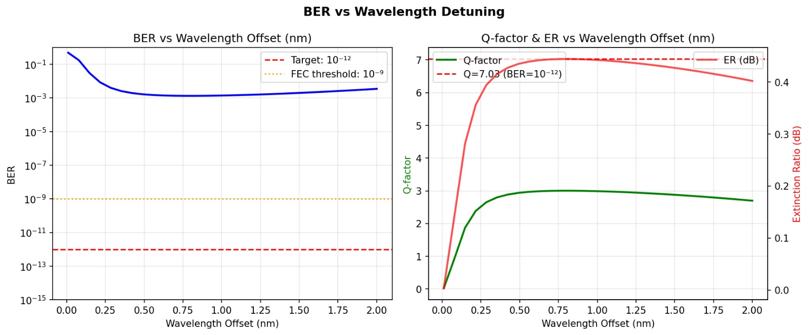
Wavelength detuning tells a similar story. Operating too close to resonance floods the receiver with noise. Moving the operating wavelength away from the notch improves signal integrity — but only up to a point, after which extinction ratio drops and BER rises again. The sweep finds the sweet spot.
9. PDK Integration — Real Process, Real Numbers
Everything above uses generic parameters — sensible defaults, but not tied to any specific fabrication process. That is fine for validating methodology. But verification only matters when it uses real physical parameters from real processes.
We chose the SiEPIC EBeam PDK — an open-source process design kit for 220nm silicon-on-insulator photonics, developed at the University of British Columbia. It includes measured compact models for waveguides, directional couplers, grating couplers, and contra-directional couplers.
Our extraction reads the PDK's XML lookup tables and PCell definitions — waveguide effective index, grating coupler loss, heater resistance, default bend radius — and maps them into our YAML configuration format. The parser reads what the process provides and writes what the verification flow consumes.
The SiEPIC process has different characteristics than our generic defaults: higher waveguide loss (3 dB/cm vs 2 dB/cm), higher grating coupler loss (4 dB vs 3.5 dB), and a TiN heater with 1200Ω resistance. These are real numbers from a real fabrication process — and they change the verification results.
SiEPIC EBeam 220nm SOI — Process-Aware Results
Tighter coupling (lower κ²) compensates for higher process loss by producing a deeper resonance notch and larger optical modulation amplitude. The framework identifies this tradeoff automatically — the kind of process-specific insight that matters for design optimization.
10. Layout to Verification — Closing the Loop
PDK parameter extraction is one step. The next question: can we go from physical layout to verification results without manual parameter entry?
We built a pipeline that starts with a GDSFactory layout — specifying ring radius, coupling gap, and coupling length — extracts the physical parameters using process-aware models, generates a YAML configuration, and runs the complete verification flow. Layout in, results out.
With a ring resonator layout (R=10μm, gap=0.2μm, coupling length=4μm) on the SiEPIC 220nm process, the layout-extracted parameters produced:
Layout-Extracted Verification — Actual Results
The results exceed the target by a wide margin — which is itself useful information. In practice, this means the design has margin that could be traded for other objectives: smaller ring radius, wider coupling gap for manufacturing tolerance, or relaxed thermal tuning requirements. The framework quantifies those tradeoffs.
11. A Real Bug — Found Only Because of Co-Sim
During development, our C gate-level engine diverged from the Python golden model. The FSM was stuck in RESET. Would not advance.
We traced it. 645 combinational gates — ANDNOT and ORNOT cells from Yosys synthesis — were missing from the C simulation kernel. Every one returned an unknown value. Those unknowns fed flip-flop enables. The entire sequential state was frozen.
But there was a second bug underneath. The gate evaluation order — the dependency sort that determines which gates compute first — had over 600 ordering violations. Gates were evaluated before their inputs were ready.
We fixed both. Clean evaluation order. Python and C engines match exactly.
This is exactly the kind of bug that shows up at silicon bring-up and takes weeks of board-level debug. We caught it because the digital controller and the optical physics were in the same simulation.
12. GPU Acceleration — Regression at Scale
One link, one temperature, one wavelength — that is a demo. Real verification means sweeping thousands of corners. We built GPU-accelerated engines for the photonic models.
| What we sweep | Scale | Speed |
|---|---|---|
| Wavelength spectrum | 1M points | 119M evaluations/sec |
| Process variation (Monte Carlo) | Thousands of corners | 6.8M samples/sec |
| Thermal transients | 100 links in parallel | 3.8M link-steps/sec |
| WDM channels | 32 channels + crosstalk | 32 channels in 16ms |
The GPU engines use the same physics as the scalar models — just vectorized across parameters. Every result is cross-checked between CPU and GPU backends. These speeds are measured on a single RTX 4060 — not a datacenter GPU.
13. What This Means for Verification Engineers
If you work in digital verification, your skills — coverage-driven methodology, fault injection, regression, systematic signoff — are directly applicable to a domain that is growing quickly.
The photonics community has brilliant physicists and optical designers. The opportunity is in bringing verification discipline to the system level — the interactions between digital controllers and photonic devices that are difficult to test in any single tool.
The mapping between domains — PLL to ring modulator, trim DAC to heater DAC, bond pad to grating coupler, thermal crosstalk between rings mirroring supply noise between PLLs — means the learning curve is shorter than you might expect.
14. Where We Are and Where We Are Going
Working Today
- 6 photonic behavioral models
- GPU-accelerated evaluation
- PhotonicLink end-to-end simulation
- Calibration FSM (RTL + gate-level)
- Mixed-domain co-sim (Python + C)
- Fault injection scenarios
- BER estimation + eye diagrams
- Single-command verification flow
- PDK parameter extraction (SiEPIC EBeam)
- Layout-to-verification pipeline (GDSFactory)
- YAML-configurable everything
Building Next
- EQWAVE-Optical waveform comparison
- HTML report generation
- Layout-to-netlist extraction (KLayout)
- Photonic DRC with intelligence
- UVM photonic VIP framework
- Multi-PDK parameter support
15. A Note on Approach
We want to be transparent about where we are and what this is. This is early-stage infrastructure. We are verification engineers learning photonics, not the other way around.
The models are behavioral — they capture the physics that matters for controller verification, not for optical device design. They complement device-level tools like Lumerical INTERCONNECT and foundry compact models, rather than replacing them. Our goal is controller and system-level verification — making sure the digital FSM and the photonic device work together correctly across temperature, process variation, and fault conditions.
The GPU benchmarks are real, measured on a single RTX 4060. The PDK integration reads real parameters from the SiEPIC EBeam process. The layout-to-verification pipeline is automated but currently supports a single ring topology — multi-ring WDM and MZI links are next.
What gives us confidence is the methodology. Coverage-driven verification, systematic fault injection, closed-loop co-simulation — these are proven disciplines. Extending them to photonics is a natural step in the same direction that semiconductor verification has always evolved: whenever a new domain becomes critical to system function, verification methodology follows.