
By early 2025 we had an architecture we believed in. The next question was the plain one. Would it become silicon. This is the account of taking that design into a full physical flow, how far it went, where it stopped, and what stopping taught us.
We were not measuring tools
We did not start this to benchmark EDA. We started it to answer one question about our own design. Could the architecture we had drawn survive placement, routing, and the physical reality of a process. Everything we did was in service of that single answer.
What we were trying to place
The design was a multi-model AI chip. One edge die running several classes of model at once: small models for quick decisions, large models where accuracy mattered, and video processing models for the streams that never stop. To keep all of that on one die inside a tight power and cost budget, the architecture placed dense on chip memory next to the compute, many SRAM hubs feeding the inference datapath, because the moment data leaves the die is the moment power and latency both rise.
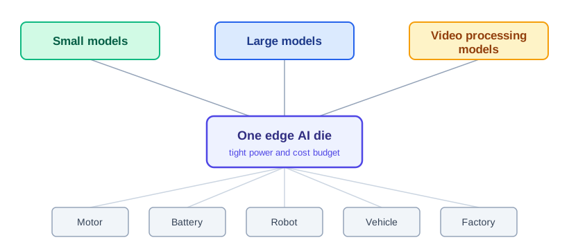
That memory density is not a detail of the design. It is the design. It is what lets several classes of model share one small die and still answer in time. We were not willing to treat it as negotiable.
The CPU we kept changing
The compute side did not settle on the first try. We began with an open, well verified RISC-V core, a capable design with packages, interfaces and a deep file tree. Our simulator at the time could not elaborate all of it cleanly, so we pushed it through synthesis into a flat gate level netlist, tens of thousands of lines of structural Verilog that ran but that we could not see inside. It worked and it was opaque.
So we dropped to a minimal core, single file, plain Verilog, no packages. It compiled everywhere and booted firmware on the first try, and it gave us a working platform to verify the peripherals against. It was scaffolding, good scaffolding, but not the processor we wanted to ship. So we built our own pipelined core. It ran, and then it met a wall that had nothing to do with the core itself. Our SoC used one bus for both instruction fetch and data access, and every time a data access stalled, the instruction fetch stalled with it. The conflict was architectural, not a bug to be found.
The answer was to stop fighting the bus. We moved to a quad core cluster where each core kept its own instruction memory and shared data through a crossbar, so the external bus carried only slow register traffic, not fetches at pipeline speed. The conflict that had cost us weeks simply did not exist in that topology. The earlier core was not wrong. It was wrong for that bus.
Open infrastructure took us to the start line
Open PDKs and open source EDA gave us a first implementation. A floorplan. A power grid. Placement. Routing. Without them, a small team would not have reached the physical flow at all, and we say that plainly. What follows is not a story about a tool falling short. It is a story about a design meeting a constraint that no amount of tooling could argue with.
We went further than a demonstrator
This was not a toy run. Roughly 275,000 standard cells. Seventy six compiled SRAM macros. A full power distribution network. Antenna repair. A clock tree. The flow did a great deal of correct work, and for a long stretch it looked like it would go all the way. The design placed. The early stages closed. The trouble arrived later, and it arrived from the geometry.
The floorplan that would not breathe
The die was a rectangle a little over fifteen square millimetres, on an open frame shuttle. Into it we had to place seventy six compiled SRAM macros, rigid blocks about 388 by 307 micrometres each, every one needing a keepout halo on all sides. Around and between them went roughly 275,000 cells of logic: the CPU cluster, the inference fabric, the bus, the peripheral decoders, the clock trees and the power switches.
SRAM macros do not negotiate. They have fixed dimensions, fixed pin sides and fixed power rails. The floorplanner has to find an arrangement where every macro sits legally, every pin faces a routing channel, and enough room remains between them for everything that connects. The placement closed. Then the clock trees went in, and the picture changed. Three clock domains meant three trees, each with its own root and its own skew budget, and each one needed routing tracks on the same layers that carried every other signal. The tracks the clocks took were tracks the buses could not.
How we verified it, stage by stage
Under all of it ran one idea we hold to. A single verification spine, the same testbench from the first RTL line down toward the extracted GDS. Not separate checks that each declare victory on their own, but one thread, so the stage where a mismatch first appears tells us the class of the problem.
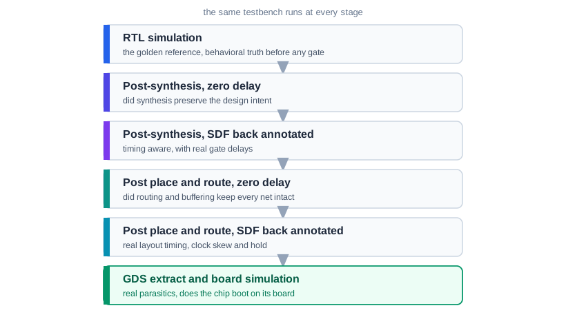
The same boot sequence, the same peripheral access, the same inference workload, run at every level. If a stage passes with zero delay but fails once delays are back annotated, the problem is timing, not logic. If post place and route breaks what post synthesis passed, routing moved or dropped a net. If the extracted layout shows an open, there is a physical break, not a coding bug. This spine kept the upper stages clean, so when the trouble came it was not in the logic. It was further down, in the physics of the routing and then in the signoff, further than most first attempts ever reach.
Where the first flow stopped
The first way we routed it was the ordinary way, the whole die at once, and it stopped. The process we were on offers five metal layers. The two lowest go mostly to the internals of the standard cells. The top layer carries the power grid that feeds the entire die. That leaves two layers in the middle to route every global signal, every clock path, and every wide bus between the memory hubs.
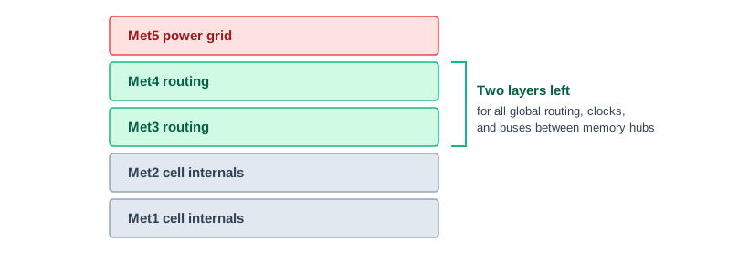
For a memory dense AI layout, two routing layers between large SRAM macros is very little room. The buses that move data between the hubs need width, and the width had nowhere to go. The router worked within the space the geometry allowed. The geometry was the wall. This was not a single mistake we could point at and correct. It was the shape of the problem: a memory dense architecture asking a thin metal stack for room it did not have.
The tools told us exactly how little room. Global routing finished in a state of overflow, with total congestion at about one hundred and forty six percent of the tracks available and the lowest usable layer called on for more than two and a half times what it could hold. Detailed routing, the stage that commits wires, reached about forty three percent before it stalled, leaving thousands of connections with no legal path. This was not a router that nearly finished and needed a nudge. It was a design asking for far more wiring than five metal layers between seventy six memory macros could ever provide.
The choice we would not make
There was an obvious way to make it route. Shrink the memory. Lower the clock. Cut the compute. Give the router room by making the design smaller. It would have worked. It would also have quietly turned our architecture into a weaker, different one, the exact thing we set out not to build.
We costed what each retreat would buy. Cutting the eight weight banks to four would free macros and the room to route, but four banks means four resident models, and the pipeline we built to switch models in one cycle would be back to reloading weights on every other pass, the exact stall the design existed to remove. Dropping the quad core cluster to a single core would free the crossbar and its instruction memories, but then inference, peripheral service and the safety monitor would run one after another on one thread, and the latency the architecture was meant to protect would grow. Halving the inference clock would relax the routing and the clock trees, and it would also halve the throughput, so the same models would take twice as long to cycle. Every option bought a routable die by giving up the reason the die existed.
So we did not cut it. We changed how we routed instead. The architecture is the point, and when a constraint asks us to give it up, the constraint is the thing to change, not the design. The right home for this die is a node with more metal, seven to nine layers, where the routing layers stay free while power sits above them, and that lives on the other side of a closed process. But we were not ready to concede the die we had, so we went looking for a way to route it that the ordinary flow did not know.
We routed it a different way
The ordinary flow routes the whole die at once, and on a die this dense it drowns. So we stopped routing the die as one thing and started routing it as many. We split it into regions, gave each region its own routing space to work in, and closed them one at a time before stitching them back together. Where the single pass had run to a hundred and forty six percent of the tracks it had, the regional pass finished with no overflow at all, in about thirteen minutes, and with fewer than five hundred repair buffers where the single pass had inserted three hundred and eighty six thousand before it gave up.
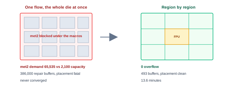
The hardest region was the floating point unit, boxed in by memory macros with almost no room to breathe. The instinct across the industry would be to cut it. We did not. We tiled the region, and when one tile stayed stuck at more than four thousand violations, we split that tile again, three ways, until every one of the eight tiles routed to zero. Regional routing inside regional routing, because the alternative was to remove the maths the chip was built to do.
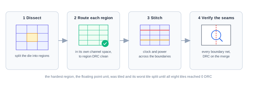
Stitching the regions back together was its own trap. A region that is clean on its own is no proof that the whole is clean. Connections went missing where the regions met, lost to name collisions in the merge, and a per region pass would never have caught it. So we added a step that did nothing but check the seams: tally every net across the boundaries, confirm each one still connected, and rerun the design rules on the merged whole before trusting any of it.
A layout, and how far it got
It worked. A finished layout came out the far end, a GDS of more than four hundred megabytes, so large that the ordinary streamer wrote an empty file and we had to generate it another way. The design rule check on the routing came back with zero violations on every signal layer. The counts that remained were the standard library markers the process waives on every shuttle, not our design. The gate level simulation passed, five of five, bit exact against the reference. And of the twelve foundry prechecks, ten came back green, an eleventh clean but not in a way we fully trusted.
For an open flow on a memory dense AI die, that is further than it is meant to go. We are not going to undersell it. We are also not going to pretend it was finished.
The check we could not close
The one that never came back green was the layout versus schematic check, the proof that the chip we drew is the chip we wired. On the full design the open source checker would run for hours, once for the better part of two days, and never return a verdict at all. When it did return, it did not point at the logic, which matched everywhere we could check it, subcircuit for subcircuit. It pointed at power and ground connections on the memory macros and a handful of nets up in the wrapper.
We chased it. We reworked the back end metal, the routing and the vias, and cut the remaining violations by more than ninety percent. The check still would not close. A layout that will not prove it matches its netlist is not a chip you submit, and this one we did not submit. That is closer to a failure to close than to a success, and we will say it that way. The design was sound as far as every check that finished could see. The flow ran out of road before the last check could.
The cost was not the failure. It was not knowing why.
Here is the part that moved us. Through all of it, the flow told us pass or fail. It did not tell us what kind of failure. Was it the floorplan, the macro placement, the power grid, the routing, the technology itself. And at the end, was a flagged violation a short in the metal or an artefact of extraction, an open power pin or a check that simply could not finish. Each points to a different fix, and the flow would not say which. So we sorted it the slow way, by hand, one theory at a time. Days went into separating the few flags that meant a dead chip from the thousands the process simply waives, work a flow that understood its own output could have done in minutes.
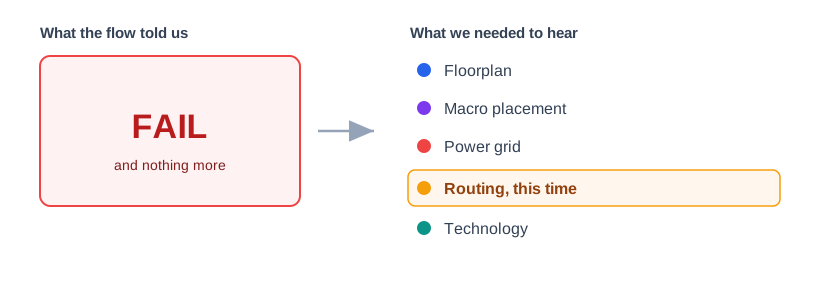
That gap is the whole thing. A flow that only says pass or fail hands the hardest question, why, back to the engineer. For a small team, that question is the entire budget.
What the verification proved, and what it did not
The design did not reach silicon. The verification still reached a conclusion. We checked the hardware against independent reference models, written from the specification rather than from the RTL, so a pass meant the design matched intent and not merely itself. A register shadow tracked every write and predicted every read. A byte comparator watched the DMA engine. A predictor checked the interrupt controller against its priority rules. And a bit exact model of the inference array recomputed the same arithmetic and compared the result cell by cell. Those checks passed. We were also plain about what that proves. It proves the design correct for the inputs we thought to try, which is weaker than proven for every input. The value is that the coverage tells us which corners are still empty, so we know the shape of what is left. All of it, the testbench, the reference models, the coverage, carries forward to the next attempt.
Where each of our tools began
There is a second story folded inside the first. Every time the flow in front of us could not do something the chip needed, we stopped and built the piece that was missing. None of it was planned as a product line. Each tool was a reaction to a specific gap, met in the order the design forced us to meet it.
| What the design needed | What the open flow left to us | The tool we began |
|---|---|---|
| RTL simulation carrying our SystemVerilog assertions, interfaces and coverage | the synthesis and simulation path did not carry SystemVerilog assertions and covergroups through intact | SystemVerilog and UVM simulator |
| Reading a waveform and tracing a signal back to the line that drives it | debug stopped at the signal, not at its cause | waveform debugger with source tracing |
| Knowing what the tests exercised | coverage lived in fragments across separate tools | coverage tool |
| Gate level netlist simulation, zero delay and SDF back annotated, at full chip scale | million gate netlists were too slow to simulate the ordinary way | gate level simulator, plus a hardware emulator for full chip runs |
| Proving the netlist still equals the RTL after synthesis and after place and route | logical equivalence sat as a separate, closed step | equivalence checking tool |
| Finding opens, floating nets and broken connectivity inside the netlist | the netlist reported pass or fail, not where it broke | netlist debug and integrity tool |
| Design for test, scan insertion and pattern generation | DFT was assumed to exist, not provided | design for test tool: scan insertion and pattern generation |
| Extracting parasitics from the GDS and booting the chip on its board | no open path took us from a finished GDS back to a chip running on a board | parasitic extraction and board level simulator |
| Routing a memory dense die the ordinary flow could not | the single pass drowned in congestion and ran the buffer count to hundreds of thousands | regional routing that solves the die in pieces and stitches it back |
| Trusting a design assembled from separately routed regions | clean in each region did not mean clean once merged | a boundary and merge verifier |
| Knowing which signoff flags mean a dead chip and which are noise | the checker reported a wall of violations without ranking them, and sometimes could not finish at all | signoff classification that separates blocking from waivable |
What we decided to build
We did not set out to build EDA in order to sell EDA. We set out to build it because we needed answers our flow could not give. Before we commit money to a node, we want to know, early, whether this architecture will route, what the power envelope is, where the timing margin sits, and when something fails, which of those it was. Not pass or fail. The category. The reason.
That is the tool we started building. Not a replacement for a commercial flow, but a flow that understands what it is doing well enough to tell us where it went wrong. And a flow that can finish, because a check that runs for days and never answers is not a check. The chip asked the question. The tools are our answer to it.
The next piece follows the question that comes straight out of this one. How do you build trust in an EDA tool with no customer history?
Our Approach
We're building systems that think about specifications the way engineers do.
We build our own in-house EDA with an intelligence layer across it. Our stack covers the full flow,
from spec to comprehensive sign-off, on tools we build and control.
Walk-in ones, walk-in zeros