
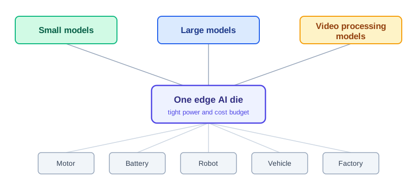
WIOWIZ began in March 2025 as a fabless team with one goal: build a multi-model edge AI chip. Not a large accelerator for a data centre, but a small, low power die meant to sit close to where data is produced. A motor housing. A battery pack. A robot joint. A vehicle cabin. A factory line.
The problem we set out to answer
Edge intelligence has a scheduling problem. A vibration signature needs one model. A current waveform needs another. A layer that combines them into a decision needs a third. In a data centre you give each model its own accelerator. At the edge you have one die, one power budget, and every model needs its answer before the next window of data arrives.
The common approach is to build one inference engine and time share it: load model A, run it, flush, load model B, run it, flush, load model C. Every switch costs a memory transfer, and at the edge that transfer is the bottleneck, not the arithmetic. We wanted to remove the switch cost, not shrink it.
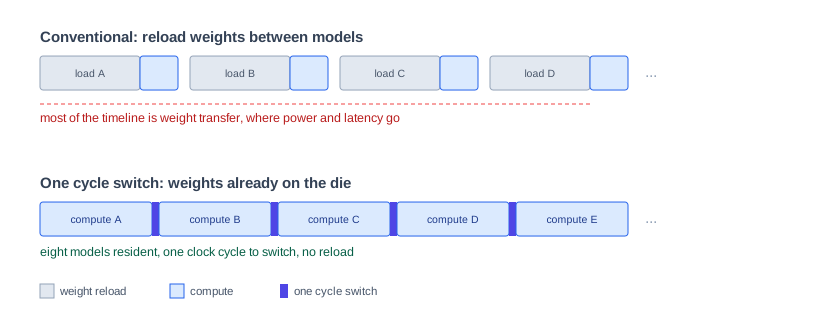
Eight models, one cycle to switch
The architecture held eight independent weight banks on the die, each holding a complete model. Switching from one model to the next was a single register write: one clock cycle, no memory transfer, no cache flush, no DMA. The compute fabric read from whichever bank was selected.
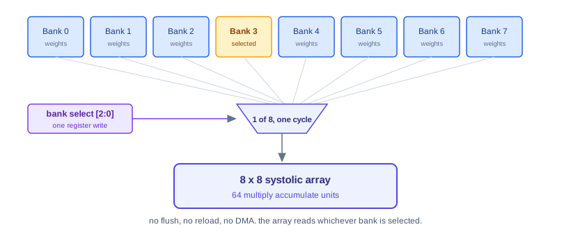
That let one die carry several models at once and run them in sequence on the same input. A motor node could score bearing wear, imbalance, misalignment and looseness on a single vibration capture, then hand the combined result to a decision model, without a weight ever leaving the die. The banks are backed by on chip memory, and the switch between them is bounded and deterministic, which is what a safety schedule needs.
Where the numbers started
The idea was clean on a whiteboard. The arithmetic made it hard. We took the design to an open 130 nanometre process, SKY130, on a shared open frame shuttle with a fixed die. The floorplan we placed into was a rectangle of about 3.17 by 4.77 millimetres, a little over 15 square millimetres, and everything had to fit inside it.
Synthesis put the logic at roughly 275,000 standard cells: the quad core CPU, the inference fabric, the bus, the peripheral set, the clock trees. The inference fabric on this validation die was a compact eight by eight array of multiply accumulate units, sixty four in all. The architecture is built to scale that to sixteen tiles, four thousand and ninety six units, at a production node. This run was about proving the fabric and the flow, not the peak number.
| Block | Function | Clock domain |
|---|---|---|
| CPU cluster | Quad core RV32IMF, local instruction memory, shared data memory | CPU |
| Inference fabric | Eight by eight systolic array, sixty four MACs, eight weight banks, one cycle switch | NPU |
| DMA | Bus master moving activations and results | CPU |
| Interrupt controller | Priority arbitration across the peripheral sources | CPU |
| Peripherals | UART, SPI, I2C, GPIO, timers, watchdog, CAN | peripheral |
| Bus fabric | Interconnect, arbiter, two clock domain crossing bridges | mixed |
| Power management | Clock gating and the reset tree | CPU |
| Self test | Built in self test for the SRAM | CPU |
| Boot memory | Startup code | CPU |
| Pad ring | IO multiplexing, level shifters, protection | - |
About 275,000 cells in all, across three clock domains.
Then came memory. The design used foundry compiled SRAM macros, hard rectangles of fixed size, 1024 words by 32 bits, four kilobytes each, about 388 by 307 micrometres of silicon with a keepout halo on every edge. The final build placed seventy six of them, for the weight banks, the CPU local memory and the activation buffers.
The constraint was not the total area. It was the shape. An SRAM macro cannot be split, rotated freely, or overlapped. Tile seventy six rigid rectangles into a 15 square millimetre die and their geometry starts to dictate the floorplan. The logic flows into whatever the macros leave behind.
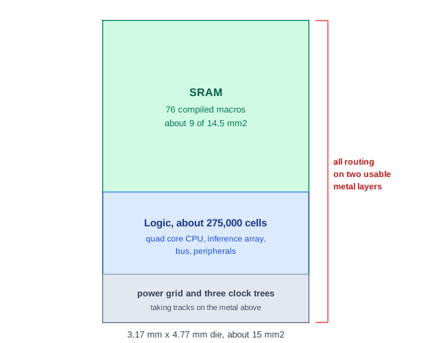
The arithmetic. Seventy six compiled SRAM macros at about 0.12 square millimetres each come to roughly nine square millimetres of memory, most of a 14.5 square millimetre core. Around 275,000 cells of logic fill much of what is left. The power grid and three clock trees take their share of the metal above. What remained for global routing was two usable metal layers, and that is where the hard part began.
Compiled memory, not generated
We used foundry compiled SRAM macros, characterised across process corners and proven in silicon, rather than macros we generated ourselves. Generated memory is flexible and free, and on paper the area looked better. But the chip was meant to become silicon on a shuttle, and a memory that does not work on a shuttle is a dead die, with no respin and no debug. The compiled macros cost money. A dead die costs more.
| Criterion | Generated by a compiler | Foundry compiled macro |
|---|---|---|
| Cost | Free | A license fee per macro |
| Configurability | Any depth and width | Fixed, one size |
| Timing models | Estimated | Characterised across process corners |
| Silicon proof | None yet | Has shipped before |
| Risk on a shuttle | Unknown, first silicon for the macro | Known |
| Our choice | This one |
A full SoC, not a bare accelerator
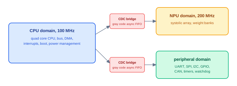
The inference fabric was the smallest part of the story. Around it sat a quad core RISC-V CPU with its own local memory, a DMA engine, boot memory, an interrupt controller, power management, and a full industrial peripheral set: CAN, SPI, I2C, UART, GPIO, timers and a watchdog. The design ran three clock domains, the CPU at 100 megahertz and the inference fabric at twice that, and every crossing between them passed through a clock domain crossing bridge built from a gray coded asynchronous FIFO. Two of those bridges carried every command and result between the CPU and the rest of the chip.
What we could not fully prove
By the time the design was stable it was a complete SoC with a novel piece at its centre, the single cycle bank switch, that no one had built before because no one had needed to. There was no compliance suite for it, no reference design to lean on, no prior silicon to compare against. Every corner case had to be invented, tested and judged by us. We wrote independent reference models that checked the hardware against the specification rather than against itself, including a bit exact model of the inference array that compared its output cell by cell. The tests passed. We were also clear with ourselves that passing the tests we thought to write is a weaker statement than proven for every input, and we kept track of where the untested corners were.
| Reference model | What it checks |
|---|---|
| Register shadow | Predicts every register read from every write |
| Byte comparator | Checks each byte the DMA engine moves |
| Priority predictor | Checks the interrupt controller picks the right source |
| Bit exact inference model | Recomputes the array output and compares it cell by cell |
Each model is written from the specification, so a pass means the design matches intent and not merely itself.
Where WIOWIZ stood
By early 2025 that is where WIOWIZ stood. A multi-model edge AI architecture with a deterministic single cycle switch at its heart. A die budget that was tight but feasible. A memory decision that traded flexibility for silicon confidence. A verification effort that was wide and still incomplete on the parts that were new. And underneath all of it, a growing set of tools the chip kept asking for, none of them planned as products, each one built because the design in front of us needed something the flow could not yet do.
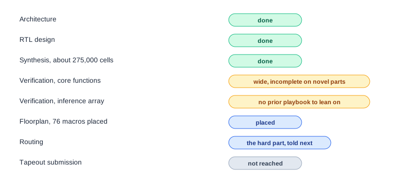
The next piece is the tapeout we did not finish.
Our Approach
We're building systems that think about specifications the way engineers do.
We build our own in-house EDA with an intelligence layer across it. Our stack covers the full flow,
from spec to comprehensive sign-off, on tools we build and control.
Walk-in ones, walk-in zeros